We use cookies to improve your online experience. By continuing browsing this website, we assume you agree our use of cookies.
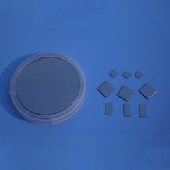
  • Semiconductor Single-Crystal Substrate Gallium Arsenide (GaAs) Crystal Wafer
1/1
  • Semiconductor Single-Crystal Substrate Gallium Arsenide (GaAs) Crystal Wafer

Semiconductor Single-Crystal Substrate Gallium Arsenide (GaAs) Crystal Wafer

Semiconductor Single-Crystal Substrate Gallium Arsenide (GaAs) Crystal Wafer
0.0 (0 Reviews)
$20.00 $10.00
Received successfully
Coupon Code
CONTINUE SHOPPING
    Please select the information you wantX
Quantity
-
+
  • Description
Semiconductor Single-Crystal Substrate Gallium Arsenide (GaAs) Crystal Wafer

GaAs is a new semiconductor material with the most in-depth research and the most extensive application after Si. It has the characteristics of high mobility, wide band gap and high-temperature resistance. It is mainly used in high frequency communication, wireless network and optoelectronic fields, such as LED illuminators, solar panels, etc. We can provide intrinsic, lightly doped and heavily doped (Si, Zn doped).
Parameter
GaAs Crystal and Substrate
Growth Method LEC,HB
Crystal Structure cube
Density 5.37g/cm3
Purity Intrinsic (99.9999%), light doping, heavy doping
Crystal Orientation Type N, < 100 > 15 °
Type P, < 100 >
Intrinsic, < 100 >
Size Φ 1″~8″ × (0.25~200)mm
Polishing Single or double sided polishing
Surface Roughness Dislocation density < 105
Encapsulation Class 100 ultra-clean bag, single or multi wafer box
Frequently Bought Together
more
Frequently Bought Together
Customer Reviews
0.0 0 Reviews
Write a review

Adding to cart succeed!

items in cart.

Total:

Requires a minimum purchase of {MinPrice}. And you still need to meet the requirements.

Proceed to Checkout Return to Shopping